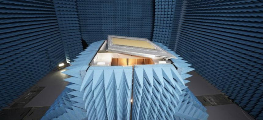
The Electronically-Scanned Multifunction Reconfigurable Integrated Sensor (EMRIS) in a Northrop Grumman testing range. Northrop Grumman


Northrop shows off new digital radar tech in first flight
Breakthroughs in design for military-specific chips are ushering new capabilities.

Northrop Grumman on Wednesday announced the successful first flight of its Electronically-Scanned Multifunction Reconfigurable Integrated Sensor, or EMRIS, aboard a U.S. military aircraft. The development paves the way for eventual deployment of new radar capability that will enable future jets to avoid a wider array of threats.
And the tech can change rapidly as the threat picture evolves.
EMRIS is an electronically scanned array, or AESA, a technology that has existed since the 1960s, but has become far more robust in the last couple of years thanks to improvements in chip design and information technology. AESAs use computers to steer radio waves, and modulate frequency and power to better avoid detection and jamming in radar systems.
But these arrays don’t develop very quickly and are extremely difficult to upgrade or change once deployed. That’s a big problem for the military, as digital electronic systems for finding or detecting waveforms have advanced quickly in the commercial world. It’s one reason why DARPA, in 2014, launched a program called Arrays at Commercial Timescales, or ACT.
“A system with static RF or analog features cannot leverage the advancements of the underlying digital electronics and, therefore, will exhibit fixed capability in an evolving threat space. It is imperative to define a path toward shorter design cycles and infield updates,” reads a DARPA BAA on the program. The goal of the program is new phased arrays that can be modified at the pace of digital electronics.
The EMIRIS tech comes out of that program. “By applying the flexibility of a digital AESA, EMRIS can perform multiple functions including radar, electronic warfare, and communications, simultaneously,” Northrop said in a statement Tuesday.
EMRIS is the result of key investments the company has made in developing new semiconductors, with foundries in California and Maryland. Defense One visited the Maryland facility in February.
During the visit, Vern Boyle, vice president of Northrop Grumman Microelectronics Center, described how differently chip design and manufacturing works in defense applications versus the commercial world. The economics are far more challenging for defense firms as Northrop needs to make very small numbers of very specific chips, which prevents them from taking advantage of the massive manufacturing plants that outfits like Taiwan’s TSMC use to make lots of chips that don’t vary much.
“You go to an Intel or you go to a TSMC [chip fabrication facility.] they're making millions and millions of chips. We need lower volume, purpose-built chips…So commercial fab might make one or two products. We make 90 products across our fabs.”
Between the two fabrication facilities, he said, Northrop makes on the order of five million chips a year for some 60 different products.
However, new technologies like digital twinning and modeling are helping accelerate the pace at which Northrop can manufacture new highly customized chips for jets, satellites, or other military platforms, he said.
“We use digital modeling, digital twins to design the chip, understand how it integrates up to the next packaging level, up onto the board level, up into the chassis level. So that when we make these custom-built parts, we can get it right the first time, right? And that reduces the cost and reduces the schedule.”